A 36 × 240 Gbps hybrid mode/wavelength division multiplexing transmitter using lithium niobate on insulator
SHANNON, CLARE, IRELAND, August 25, 2026 /EINPresswire.com/ -- Announcing a new publication from Opto-Electronic
Press Release Disclaimer: This is a press release distributed through the XPR Media network. It has not been independently verified by our newsroom.

SHANNON, CLARE, IRELAND, August 25, 2026 /EINPresswire.com/ — Announcing a new publication from Opto-Electronic Advances; DOI 10.29026/oea.2026.250341.
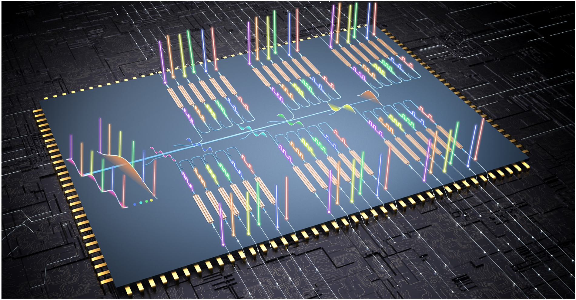
A research team from Zhejiang University, China has achieved a major breakthrough in thin-film lithium niobate integrated photonics, developing a mode/wavelength hybrid multiplexing optical transmitter chip capable of an ultrahigh transmission capacity of 8.64 Tbps for next-generation optical communications.
Driven by the rapid advancement of artificial intelligence, big data and cloud computing, global data traffic is exploding at an annual growth rate of approximately 25%, imposing severe capacity bottlenecks on conventional optical interconnection technologies. Integrated optoelectronic chips with higher speed, lower power consumption and smaller footprint are urgently demanded for long-haul backbone networks, short-reach data center interconnections, as well as chip-scale optical interconnects.
Silicon photonics stands as a mainstream integrated photonic platform with merits for large-scale manufacturing, yet it suffers inherent drawbacks in electro-optic modulation: high waveguide loss, severe nonlinear interference and limited electro-optic bandwidth, which hinder its capability to support ultrahigh-speed modulation beyond 100 Gbps per channel. Lithium niobate (LN), by contrast, serves as an ideal material for high-speed electro-optic modulators owing to its giant electro-optic coefficient, ultra-low propagation loss and broad transparent window. Particularly, the maturation of lithium niobate on insulator (LNOI) thin-film technology enables the fabrication of subwavelength waveguides on LN substrates with CMOS-compatible processes, reshaping the technical roadmap for high-speed integrated optoelectronics.
To further break the upper limit of single-channel data rate, multidimensional multiplexing technologies are indispensable. Wavelength division multiplexing (WDM) expands transmission capacity via distinct wavelengths, while mode division multiplexing (MDM) utilizes different spatial modes for capacity scaling. Their combination enables “dimensional multiplication” within a single waveguide. Nevertheless, the crystalline anisotropy of LNOI materials gives rise to severe mode hybridization. Meanwhile, designing on-chip wavelength division multiplexing devices with high precision and flat-top response poses formidable challenges. These issues have long restricted the development of large-scale multidimensional hybrid multiplexing on the LNOI platform.
This work proposes a lithium niobate on insulator (LNOI) hybrid mode/wavelength division multiplexing transmitter chip. Targeting the capacity demands of high-speed optical communications in the era of big data and artificial intelligence, it achieves practical and critical performance improvements based on existing integrated photonic technologies, offering a viable chip-scale solution for high-density, high spectral-efficiency optical transmission. By combining six modes and six wavelengths, the scheme generates 36 independent channels. Each channel supports 240 Gbps transmission, yielding an aggregate capacity of 8.64 Tbps, which represents the state-of-the-art performance among lithium niobate integrated optical transmitter chips and effectively alleviates the capacity limitations of conventional single-mode and single-wavelength transmission.
In terms of mode manipulation, this study adopts Z-propagating LNOI waveguide structures to physically suppress mode hybridization of lithium niobate, realizing stable multiplexing and demultiplexing of six modes from TE₀ to TE₅. The designed mode multiplexer relies on an adiabatic coupling structure, featuring broad operating bandwidth and favorable fabrication tolerance. Measured results show an insertion loss below 0.3 dB and inter-mode crosstalk less than −15 dB, delivering a stable and reliable core building block for on-chip mode division multiplexing (MDM).
For wavelength multiplexing, this work innovatively adopts a cascaded Fabry–Pérot (F-P) cavity structure. It successfully addresses the challenges including difficult phase control and limited free spectral range suffered by conventional wavelength-selective devices originating from LNOI crystalline anisotropy, and achieves dense wavelength division multiplexing (WDM) filtering with flat-top response.
The fabricated filter exhibits a 3 dB bandwidth of ~1.8 nm. Its channel spacing follows the ITU-T standard of 400 GHz (3.2 nm). Benefiting from low insertion loss and effective crosstalk suppression, the device guarantees reliable transmission quality for high-speed signals and maintains compatibility with existing optical network infrastructure.The integrated lithium niobate Mach–Zehnder modulators on the chip exhibit outstanding performance, featuring a 3 dB electro-optic bandwidth exceeding 67 GHz and a low half-wave voltage-length product, enabling efficient and high-speed modulation. Experiments successfully demonstrate the modulation of 120 GBaud OOK and PAM4 signals. Clear and well-opened eye diagrams are obtained for all 36 channels without obvious inter-symbol interference, verifying the reliable transmission capability of the system.
The final chip realizes parallel transmission over 36 independent channels consisting of 6 modes × 6 wavelengths, with a single-channel data rate of 240 Gbps and an overall system capacity of 8.64 Tbps. All specifications are rigorously verified via experiments.
Keywords: lithium niobate, transmitter, wavelength division multiplexing, mode division multiplexing, modulator
# # # # # #
The Silicon Integrated Nanophotonics Group (SING) at Zhejiang University has long dedicated itself to the research of high-performance, high-integration silicon-based integrated photonic devices and chips, as well as their applications in optical communications and optical interconnections, yielding abundant research achievements. The group has published more than 300 papers in top journals including Nature, Nature Communications, Light: Science & Applications and Optica, accumulating over 15,000 citations. It has received prestigious awards such as the First Prize of China Optical Science and Technology Award, the First Natural Science Award of Chinese Society for Optical Engineering, the First Prize of Zhejiang Provincial Natural Science Award, and the Wang Daheng Optics Award, enjoying prominent international influence.
The team comprises core researchers including recipients of the National Science Fund for Distinguished Young Scholars, Excellent Young Scientists Fund, and national young high-level talents. It currently hosts over 100 members including researchers, PhD and master’s students. Many of its alumni have been selected for national talent programs and awarded honors related to outstanding doctoral dissertations. Targeting major national demands such as data centers and 5G communications, the group presides over key national projects including the National Key R&D Program of China and conducts in-depth industry-university-research collaborations. Furthermore, it maintains close partnerships with world-leading research groups from the University of California, Santa Barbara (UCSB), Ghent University (Belgium), and other institutions. Relying on the Joint International Research Laboratory of Photonics under the Ministry of Education, the group comprehensively promotes internationalized research and talent training.
# # # # # #
Opto-Electronic Advances (OEA) is a high-impact, open access, peer reviewed SCI journal with an impact factor of 22.4 (Journal Citation Reports 2024). OEA has been indexed in SCI, EI, DOAJ, Scopus, CA and ICI databases, and expanded its Editorial Board to 41 members from 17 countries.
# # # # # #
More information: http://www.oejournal.org/oea
Editorial Board: http://www.oejournal.org/oea/editorialboard/list
All issues available in the online archive (http://www.oejournal.org/oea/archive).
Submissions to OEA may be made using ScholarOne (https://mc03.manuscriptcentral.com/oea).
ISSN: 2096-4579
CN: 51-1781/TN
Contact Us: oea@ioe.ac.cn
Twitter: @OptoElectronAdv (https://twitter.com/OptoElectronAdv?lang=en)
WeChat: OE_Journal
# # # # # #
Zhu MY, Wang WH, Ma RT et al. A 36 × 240 Gbps hybrid mode/wavelength division multiplexing transmitter using lithium niobate on insulator. Opto-Electron Adv 9, 250341 (2026). DOI: 10.29026/oea.2026.250341
Opto-Electronic Advances Editorial Office
Opto-Electronic Advances
+86 591 2286 1222
email us here
Legal Disclaimer:
EIN Presswire provides this news content “as is” without warranty of any kind. We do not accept any responsibility or liability
for the accuracy, content, images, videos, licenses, completeness, legality, or reliability of the information contained in this
article. If you have any complaints or copyright issues related to this article, kindly contact the author above.

Media gallery